Thank you very much George, it's exactly what I needed. I wonder where you've found it and why couldn't I? 
Posts made by Aero
Several EVB J2 connector pin/signal/net NAMES couldn't be found in the OpenIMU330BI Pin definitions document. Please clarify (pin by pin) - which OpenIMU330BI pin corresponds to every pin of the J2 EVB connector?
Thank you in advance.
Thank you but I do not need the pinout, I rather need the connections map from the SMD/BGA module to the J2 interface connector (or the OpenIMU330BI EVB schematics).
So the "small OpenIMU330BI-evb" schematics will answer all of my current questions. Please provide me/others with one in case I'm not alone who develops own custom OpenIMU330BI PCB.
Thank you in advance.
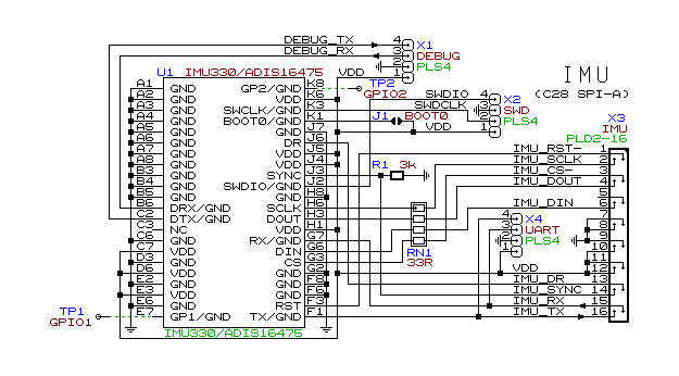
Here is my custom PCB schematics:

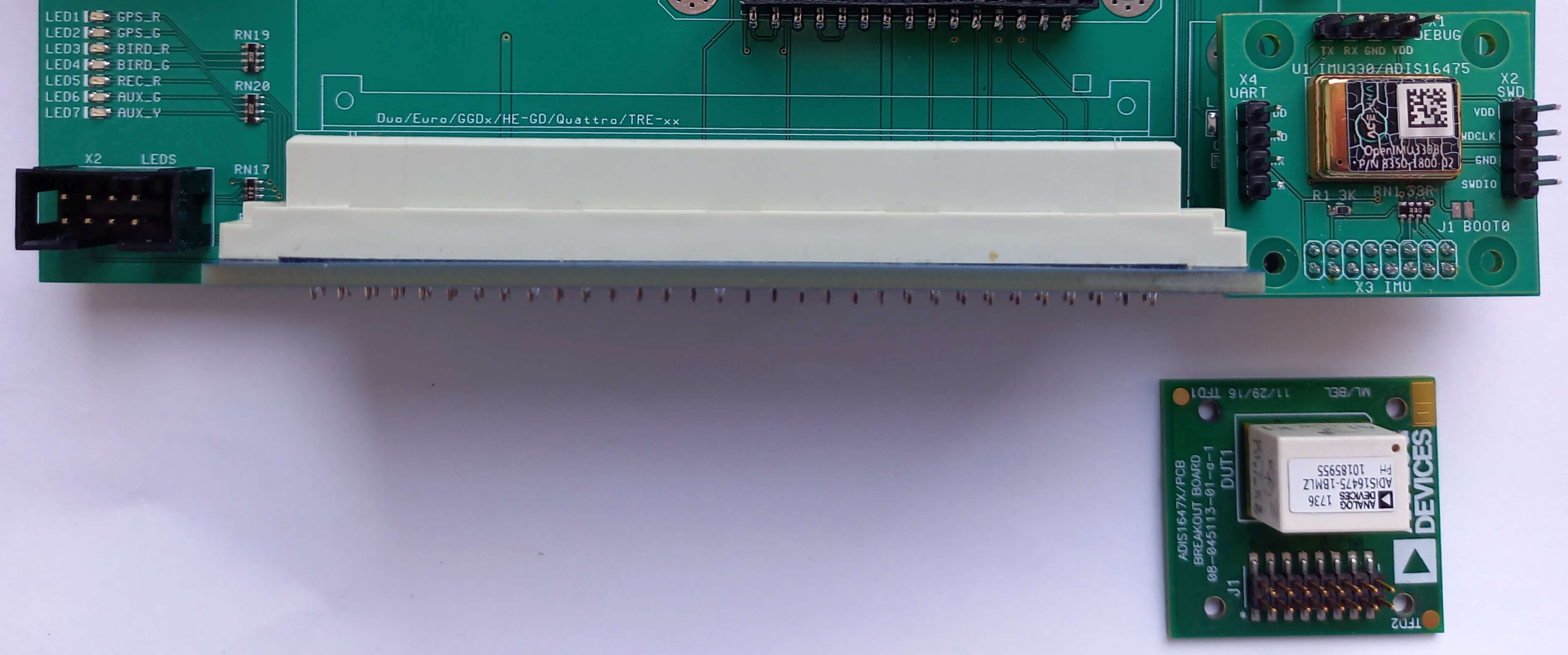
OK. For my needs I have developed a custom PCB similar to your 330BI EVB, with 16 pin connector compatible with the one on the Analog Devices ADIS16475EVB - to be able to use either ADIS or OpenIMU interchangingly. Please see the attached image.

This did not answer my question above - "Please provide more detailed info regarding functions of the GPIO1 (E7), GPIO2 (K8) and BOOT0 (K1) pins."
I meant the EVB schematics, not the module pinout. I need to know how the BGA module is connected to the EVB resources, pin by pin. Thank you.
The schematics supplied at https://openimu.readthedocs.io/en/latest/330BI/EVB-OpenIMU330BI.html shows OpenIMU300 instead of OpenIMU330, along with a totally wrong module pinout (not SMT/BGA)
It shows the 330RI pinout instead of 330BI. Please fix this and provide more detailed info regarding functions of the GPIO1 (E7), GPIO2 (K8) and BOOT0 (K1) pins. Which GPIO pin is used to select SPI or UART interface?