It shows the 330RI pinout instead of 330BI. Please fix this and provide more detailed info regarding functions of the GPIO1 (E7), GPIO2 (K8) and BOOT0 (K1) pins. Which GPIO pin is used to select SPI or UART interface?
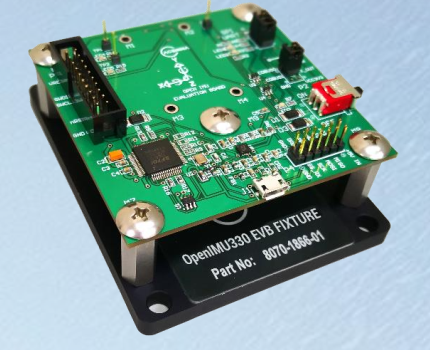
OpenIMU330BI EVK documentation is incorrect


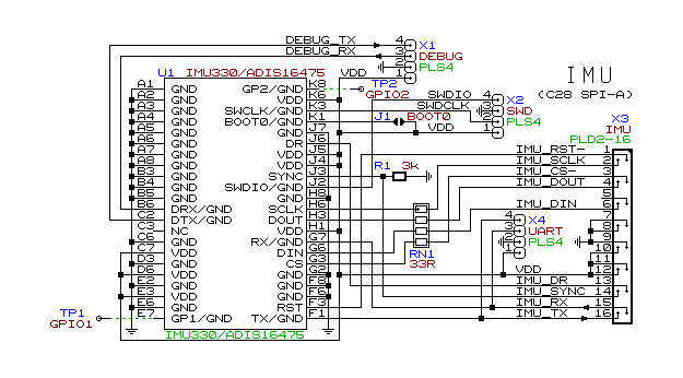
J6 PB5 DR O Data ready signal
pls refer to SPI chapter: https://openimu.readthedocs.io/en/latest/software/SPImessaging.html#openimu-spi-messaging-framework
OpenIMU supports a SPI interface for data communications as a one of the choices. To enforce SPI interface mode ‘Data Ready’ signal needs to be forced HIGH of left unconnected on system startup. OpenIMU SPI interface signals described here.
OpenIMU operates as a slave device.
This did not answer my question above - "Please provide more detailed info regarding functions of the GPIO1 (E7), GPIO2 (K8) and BOOT0 (K1) pins."
BOOT0: support build in bootloader. https://openimu.readthedocs.io/en/latest/330BI/evb_330BI_FW_update.html#using-built-in-mcu-bootloader
IO2 and IO3 is used to show internal IMU data preparing status.
hope helpful for you, could you tell us why you need the info and what is your target now? then we can supply support correspondingly.
"It shows the 330RI pinout instead of 330BI.", i think you want to say OpenIMU300ZI instead of 330BI in below link:
https://openimu.readthedocs.io/en/latest/330BI/EVB-OpenIMU330BI.html#openimu330bi-eval-kit
yes, here need to be upgraded(borrow 300ZI wrong pic).
for OpenIMU330BI, it is a chip product, pin-out pls refer to Pinout chapter:
https://openimu.readthedocs.io/en/latest/330BI/pinout.html#openimu330bi-pinout-and-function-descriptions
In 330BI evk, what we used is a small OpenIMU330BI-evb(similar with 300ZI) not 330BI-chip, sorry for not clear text in EVK chapter, the small evb is used to do quickly evaluation of performance and function in customer side(because 330bi chip is difficult to evaluate it without welding to PCB).
so, 330BI is one chip product.
330bi-evb is another module which have 20 pins, 330BI-evk include: big PCB developing board, 330bi-evb, ST-LINK debugger and micro-usb, and so on.
OK. For my needs I have developed a custom PCB similar to your 330BI EVB, with 16 pin connector compatible with the one on the Analog Devices ADIS16475EVB - to be able to use either ADIS or OpenIMU interchangingly. Please see the attached image.
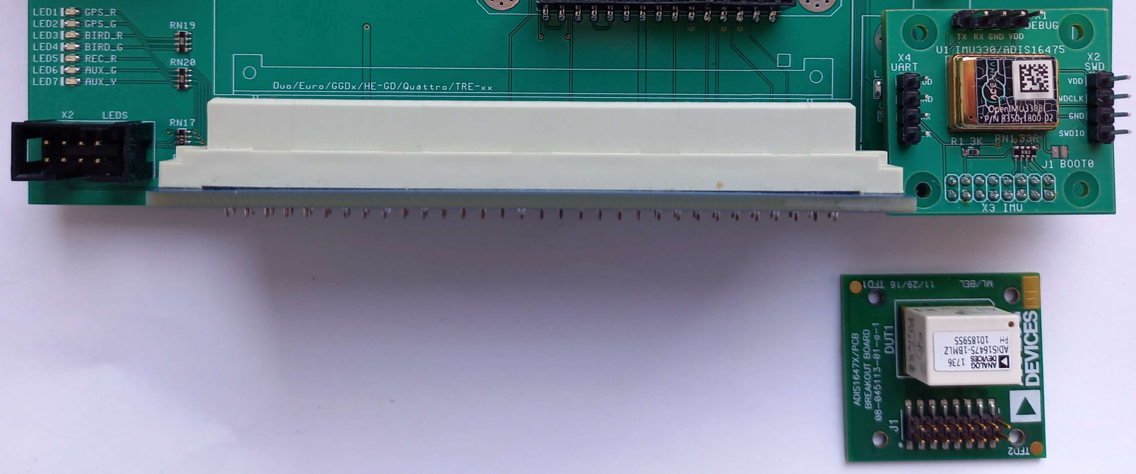
So the "small OpenIMU330BI-evb" schematics will answer all of my current questions. Please provide me/others with one in case I'm not alone who develops own custom OpenIMU330BI PCB.
Thank you in advance.
Hello, the pin definition of 330BI EVB can be referred to here: https://openimu.readthedocs.io/en/latest/300ZI/pinout.html#connector-pinout-including-gps-sensor-interface.
If you have any further questions, please contact me. My email is sliu@aceinna.com.
Thank you but I do not need the pinout, I rather need the connections map from the SMD/BGA module to the J2 interface connector (or the OpenIMU330BI EVB schematics).
Several EVB J2 connector pin/signal/net NAMES couldn't be found in the OpenIMU330BI Pin definitions document. Please clarify (pin by pin) - which OpenIMU330BI pin corresponds to every pin of the J2 EVB connector?
Thank you in advance.

@Aero Hi,you can refer the pic below of pin by pin from J1 to J2.
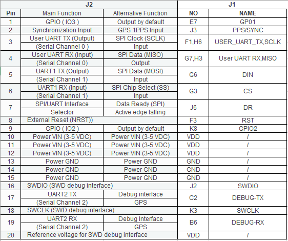
Hope this can help you .
")